Advance Digital Design
Reference Book
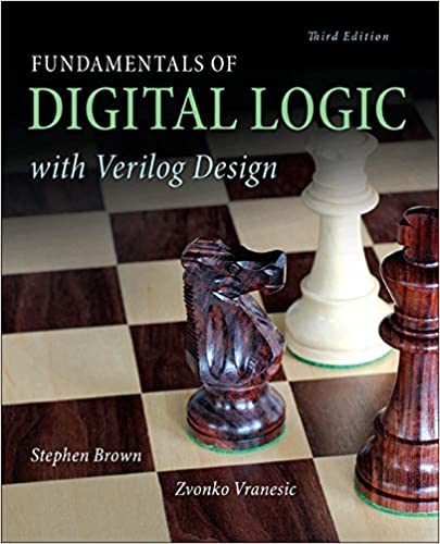
Stephen Brown, and Zvonko Vranesic
"Fundamentals of Digital Logic with Verilog Design"
3rd Edition, McGrawHill, 2014
Software
- Quartus Prime Lite Edition (Link) 24.1 or newer

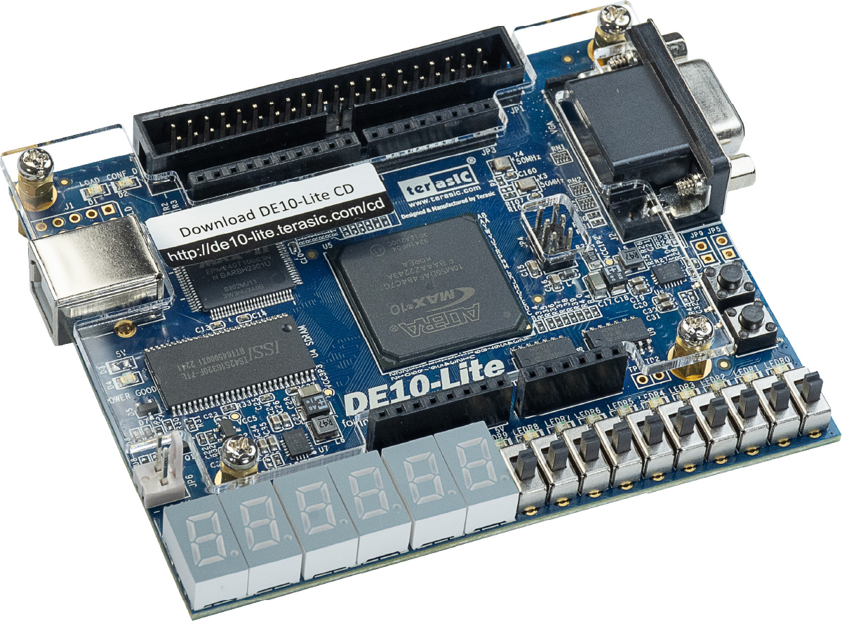
- Board: DE10-Lite (Link)
Course Goals
- Design of logic machines.
- Finite state machines, gate array designs, ALU and control unit designs, microprogrammed systems.
- Hardware design of digital circuits using SSI and MSI chips.
- Top-down design, modeling, implementation and testing of actual digital design systems hardware.
- Simulation of circuits using VHDL and hardware implementation.
Course Modules
- Module 1 - Introduction to Logic Circuits
- Module 2 - Number Representation and Arithmetic Circuits
- Module 3 - Combinational Circuit Building Blocks
- Module 4 - Flip-Flops, Registers, and Counters
- Module 5 - Synchronous Sequential Circuits
- Module 6 - Simple Processor
- Module 7 - Optimized Implementation of Logic Functions
- Module 8 - Asynchronous Sequential Circuits
- Support Module A - VERILOG Reference
- Support Module B - Implementation Technology